Introduction
Many student makers struggle with the jump from breadboard to real-world hardware. You've built circuits on a breadboard, tested your ideas, and watched LEDs blink to life — but how do you turn that tangle of jumper wires into a permanent, professional circuit board?
A PCB prototype is an early, testable version of a printed circuit board that lets you validate your electronic design before committing to full production. This guide is for teens and first-time hardware builders ready to move beyond breadboards and build something real.
Learning PCB prototyping is foundational to any serious STEAM project. It transforms you from passive learner to active builder, giving you hands-on skills that engineering universities recognise and value. The IECA describes maker portfolios as "a powerful way to differentiate yourself in the increasingly competitive admissions landscape" — and a working PCB prototype is one of the strongest portfolio pieces you can submit.
Here, you'll learn how PCB prototyping works, what tools and software you need, how to navigate your first design, and how to get boards manufactured — even on a student budget.
TL;DR
- A PCB prototype validates your circuit design before mass production
- Follow this workflow: define requirements → schematic → layout → fabrication → test → iterate
- Free tools like KiCad and EasyEDA make PCB design accessible to beginners
- Most student projects need 2–3 prototype iterations before the board works reliably
- The biggest mistakes happen during schematic and layout — small errors there tend to cause real physical failures
What Is PCB Prototype Design?
A printed circuit board (PCB) is "a laminated sandwich structure of conductive and insulating layers" with copper traces that electrically connect components like microcontrollers, resistors, capacitors, and LEDs. In practice, it's a flat board made of insulating material (usually FR4 fiberglass) with copper pathways that route power and signals between components.
A prototype is your first functional physical attempt at that design. It's not the final product, but a working model built to test whether your concept works as intended. Prototypes catch errors, validate assumptions, and help you iterate toward a reliable design.
Breadboard vs. PCB
Breadboards are temporary and reusable, making them ideal for quick concept testing. Components plug into spring-loaded sockets without soldering — no commitment required. But breadboards have real limits:
- Fragile: components fall out if the board is shaken or moved
- Low-current only: not reliable above 1 amp
- Not permanent: unsuitable for anything beyond a workbench experiment
A PCB prototype is permanent, compact, and manufacturable. Once you've validated your concept on a breadboard, a PCB is the natural next step — cleaner, more reliable, and ready to share or manufacture.
Why PCB Prototyping Matters for Student Innovators
From Abstract to Tangible
Prototyping transforms abstract ideas into testable, tangible objects — a critical mindset shift for students used to working in simulations or on paper. A 2023 study referenced by IEEE found that prototyping and rework account for approximately 43% of hardware project budgets, and teams that prototype early reduce development errors significantly.
Physical prototyping reveals errors invisible in software. Material properties can vary by as much as 15% from nominal datasheet values, and simulation cannot replicate tolerance stack-up, vibration, or humidity effects. Real electricity through real copper exposes real problems.
What Goes Wrong When You Skip Prototyping
Students who skip proper prototyping encounter:
- Components placed incorrectly or with wrong footprints
- Copper traces too thin for current requirements, causing overheating
- Power distribution issues and ground loops
- Signal interference and noise
- Reversed polarity on polarised components
Each of these failures costs time and money to fix after fabrication — which is exactly why prototyping is a skill, not an afterthought.
A Core Maker Skill
PCB prototyping isn't just for professional engineers. It's how student innovators build documented hardware projects that hold up in competitive university applications — and gain the hands-on confidence that comes from actually shipping something.
MIT's Engineering Advisory Board reviews maker portfolios. Stanford, Cambridge, and IITs look for students who have built tangible hardware. A documented PCB project spanning concept sketch, schematic, layout, fabrication, and testing does something a grade transcript can't: it shows reviewers exactly how you think and build.
What that looks like in practice:
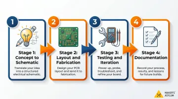
- Concept to schematic: Translating an idea into a working circuit diagram
- Layout and fabrication: Placing components, routing traces, ordering boards
- Testing and iteration: Debugging real failures with real tools
- Documentation: Writing up decisions so others (and future you) can follow the process
How PCB Prototype Design Works: Step-by-Step
PCB prototyping is a cyclical process: design → build → test → revise. It's not a straight line. Most teams consider 3–4 prototype spins normal, though industry leaders using simulation aim for 1–2.
Each step produces a specific output that feeds into the next. Skipping steps is the most common reason student prototypes fail.
Step 1: Define Your Idea and Requirements
Before opening any design software, clearly define:
- Function: What does the board need to do?
- Components: What parts will it need (microcontroller, sensors, LEDs, etc.)?
- Power: What voltage and current does it require? Battery or mains powered?
- Size and constraints: Does it need to fit inside a specific enclosure or mounting point?
Example: A soil moisture sensor that triggers an LED alert when soil is dry. Requirements: ESP32 microcontroller, capacitive moisture sensor, red/green LEDs, 3.3V operation, USB-C power input, fits inside a 5×7cm enclosure.
Step 2: Draw Your Schematic
A schematic is a symbolic diagram of how all components are electrically connected — not a physical layout, but a logical blueprint.
Tools like KiCad or EasyEDA let you place component symbols (resistors, capacitors, ICs) and draw "nets" (connection lines) between them. The schematic defines the circuit's electrical behaviour: how current flows, what connects to what, which pins carry signals.
Critical: Errors in the schematic get physically built into the board. A missed connection or wrong component value becomes a real defect later.
Before moving to layout:
- Run an Electrical Rules Check (ERC) in your EDA tool
- Have a peer or mentor review the schematic independently
Step 3: Design the PCB Layout
The EDA software converts your logical schematic into a physical board. Now you're placing component footprints — the real physical sizes and pad patterns for each part — and routing copper traces between them.
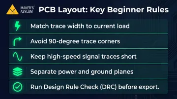
Key beginner rules:
- Keep trace widths appropriate for current load (thicker traces for power, thinner for signals)
- Avoid 90-degree corners on traces (use 45-degree angles for easier routing)
- Keep high-speed signals short to reduce interference
- Separate power and ground planes clearly
- Always run a Design Rule Check (DRC) before exporting files
KiCad's DRC "looks for design mistakes like mismatches between the schematic and layout, copper regions that have insufficient clearance or are shorted together, and tracks that do not connect to anything". Unresolved DRC errors cause manufacturing defects.
Step 4: Get It Fabricated
Export Gerber files from your EDA tool. Gerber is "the de facto standard for PCB design data transfer", maintained by Ucamco and accepted by all manufacturers.
Upload your Gerber files to an affordable PCB fabrication service. JLCPCB offers PCB prototypes starting at ₹165 ($2) for 5 boards with 24-hour turnaround, making physical prototyping financially accessible to students.
Note: You receive bare PCBs. Components still need to be sourced separately and soldered (by hand for beginners, or via assembly services for advanced projects).
Step 5: Test, Debug, and Iterate
Power the board carefully:
- Use a current-limited power supply
- Check voltages at key points with a multimeter
- Test individual subsystems before full integration
Common first-boot issues students encounter:
- Wrong component footprint (part doesn't fit pads)
- Missed connection (forgot a trace in layout)
- Reversed polarity (LEDs or capacitors installed backward)
- Insufficient trace width (trace overheats or burns)
Debugging is a skill built through practice. Each failure points to something specific — a routing mistake, a wrong footprint, a power rail issue. You fix it, spin another version, and the next board is better.
At Maker's Asylum, students work through this iterative cycle during their Innovation School residency — moving from ideation to functional prototypes, documenting each revision and building real problem-solving instincts along the way.
Tools, Software, and Resources Every Student Maker Needs
EDA Software
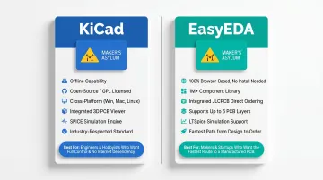
KiCad (recommended for offline work and full control):
- Free, open-source (GPL v3+), cross-platform (Windows, macOS, Linux)
- Current stable version: 10.0.1
- Features: schematic capture, PCB layout, 3D viewer with raytracer, SPICE simulation, Gerber export
- Industry-respected and used professionally
- Download at kicad.org
EasyEDA (recommended for browser-based workflow):
- Free, runs in any HTML5 browser (Chrome/Firefox recommended)
- Access to 1,000,000+ public component libraries
- Integrated ordering: export and order directly from JLCPCB/LCSC within the tool
- Features: schematic, PCB layout (up to 6 layers), DRC, LTSpice simulation, 3D view
- Start at easyeda.com
Both tools output standard Gerber files accepted by all manufacturers. Choose KiCad if you want deep control and offline capability. Choose EasyEDA for the fastest path from design to ordered board.
Physical Tools for Hands-On Work
- Soldering iron (temperature-controlled, 60W minimum)
- Multimeter (for voltage, continuity, and resistance checks)
- Oscilloscope (a basic USB oscilloscope is enough to start — see Tektronix's oscilloscope basics guide for how to read voltage over time for signal analysis)
- Helping hands or PCB holder
- Solder and flux (lead-free solder for safer use)
- Desoldering pump or wick (for fixing mistakes)
If buying all of this upfront isn't practical, a makerspace solves that immediately. Maker's Asylum's 10,000+ sq ft facility in Moira, Goa gives students access to all of this equipment, plus mentorship from experienced makers who guide you through the whole process.
Component Libraries and Datasheets
KiCad and EasyEDA come with built-in component libraries, but you should also learn to read a component datasheet. Datasheets tell you:
- Pin assignments (pinout diagrams)
- Voltage and current ratings
- Physical dimensions and footprint specifications
- Electrical characteristics
Most first-time layout mistakes — wrong footprints, swapped pins, over-voltage components — trace back to skipping the datasheet. Make it a habit before placing any component.
Affordable Fabrication Services
Once your design is ready, getting boards made is straightforward and inexpensive. JLCPCB offers student-friendly pricing: 1–8 layer PCBs starting at ₹165 ($2) for 5 boards, with production completed in as little as 24 hours. Other accessible services include PCBWay and OSH Park.
Basic process:
- Export Gerber files from KiCad or EasyEDA
- Upload to fabricator's website
- Specify layers, dimensions, solder mask colour, surface finish
- Pay and wait (typically 3–7 working days including shipping)
- Bare boards arrive; you solder components yourself
Common Mistakes and Misconceptions in Student PCB Prototyping
Mistake 1: Skipping the Schematic Review
Many students rush from schematic to layout without checking for:
- Unconnected pins (floating inputs or outputs)
- Missing power symbols (VCC, GND)
- Wrong component values (1kΩ instead of 10kΩ)
- Logical errors in circuit design
Fix: Spend 10 minutes reviewing your schematic. Ideally, ask a peer or mentor to check it. This prevents hours of debugging after fabrication.
Mistake 2: Incorrect Component Footprints
The schematic symbol and the PCB footprint are two different things. Students often select a component in the schematic without verifying that the footprint matches the physical part they've ordered — meaning a resistor specified as 0805 (2mm × 1.25mm) simply won't fit pads designed for 0603 (1.6mm × 0.8mm).
Fix: Always cross-check footprint dimensions against the component datasheet. Measure your physical parts if unsure.
Mistake 3: Ignoring Design Rule Checks (DRC)
DRC is built into every EDA tool. According to ProtoExpress's PCB DRC guide, it "identifies design errors that may lead to manufacturing defects and impact the reliability of your board." DRC flags:
- Power/ground shorts
- Insufficient spacing between traces
- Pads not connected per netlist
- Drill holes too close to traces
Many beginners ignore DRC warnings or clear them without understanding them.
Fix: Resolve every DRC error before exporting Gerber files. If you don't understand a warning, research it or ask a mentor — don't just dismiss it.
Mistake 4: Confusing the Prototype with the Final Product
Students sometimes treat the first working prototype as complete. A prototype is a test vehicle. It will likely need 2–3 iterations to address:
- Signal integrity issues
- Power distribution noise
- Component placement problems (mechanical fit, thermal management)
- Usability improvements discovered during real-world testing
Fix: Plan for iteration. Budget time and money for at least two fabrication cycles. Treat your first board as a learning tool, not a finished product.
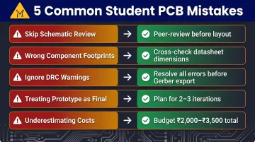
Mistake 5: Underestimating Lead Times and Full Cost
Students often calculate only the PCB fabrication cost (₹165–₹800 for small boards), forgetting:
- Component costs (₹500–₹2,000 depending on complexity)
- Shipping fees (₹300–₹800 for international orders)
- Time for iteration (1–2 weeks per cycle including fabrication and shipping)
Fix: Source components before ordering the board. Plan for at least two fabrication cycles in your project timeline. Budget ₹2,000–₹3,500 total for a complete two-iteration student project.
Frequently Asked Questions
What is a PCB prototype?
A PCB prototype is an early, testable version of a printed circuit board built to validate a design's functionality before mass production. It lets designers catch errors and make improvements at low cost.
What is the difference between a prototype PCB and an assembly PCB?
A prototype PCB is a bare or partially assembled board made in small quantities (5–10 boards) specifically for testing and iteration. A PCBA (assembly PCB) is a fully assembled board with all components soldered, typically produced at scale for a final product.
What is a prototype in design?
In design, a prototype is any early working model created to test ideas, validate performance, and surface problems before committing to final production. The goal is to learn fast and improve cheaply — before costs and complexity scale up.
What are the 5 stages of prototyping?
The five stages are: (1) define requirements, (2) design/schematic, (3) build/fabricate, (4) test and evaluate, (5) iterate and refine. In PCB prototyping, these stages often repeat in cycles until the design is stable.
What are the 4 types of prototypes?
The four main types are proof-of-concept, functional prototype, EVT sample (engineering validation), and DVT sample (design validation for production readiness). Most students work within the first two — proving the idea works, then proving it works well.
What are the 7 types of PCB testing methods?
The main methods are visual inspection, continuity/electrical testing, in-circuit testing (ICT), functional testing, flying probe testing, automated optical inspection (AOI), and X-ray inspection. For students, visual inspection, continuity testing, and functional testing are the most accessible starting points.